I originally blogged about my initial attempts at implementing IoT switches and the debugging process of V1 on my old blog. If you would like to view it you can find it here.
In this post, I will discuss the entire process of designing and implementing IoT switches that are fully compatible with Home Assistant and Google Home. The schematics, YAML and automation scripts can be found on the GitHub repository here.
Without further ado, let’s begin!
Project Goals and Requirements:
The goal of this project was to create a PCB that could switch up to 4 220VAC loads both remotely (via IoT) and locally (via a button panel) and that could fit into the standard UK switch box.
Additionally, I was inspired by the switch panels in condominiums and hotels I had visited that featured LED buttons that would light up when the switch was in the “OFF” position and vice versa, presumably to assist users in finding the light switch in the dark. As such, I decided to incorporate this element into this project, adding on an additional requirement.
Initial Implementation Ideas:
Given the requirements to switch high voltage loads, it was quite obvious that mechanical relays would be the go-to component for achieving the switching.
Having recently installed Home Assistant on a Raspberry Pi 4, I decided to use ESPHome as the firmware of the project. ESPHome offers a quick and intuitive setup, with the OTA uploading of code being a major plus, saving me the headache of prying open the switchboxes just to update the code (not to mention turning off the breakers and checking for safety). The only downside of ESPHome was that WiFi is generally a more power hungry mode of telemetry than other methods (such as NRF24L01 modules). However this downside would was inconsequential as the majority of the power would be consumed by powering the relay (a single SRD-05VDC relay consumes around 70-100mA of current in the “ON” state which is comparable to an ESP8266’s peak current consumption. Each switch needed to support up to 4 relays). Therefore, I intended to power the device from a power supply regardless of which communication method was used.
Version 1:
The first version of my implementation of IoT switches failed spectacularly. In hindsight, there was a tonne of design flaws that led to its catastrophic failure. Nonetheless, V1 provided a great learning platform for learning from my mistakes.
The first problem I encountered was the fact that there were simply not enough GPIO pins on the ESP8266 to fulfil the requirements of the PCB. The breakdown of the total number of pins is as follows:
| Function GPIO was required for | Total number of GPIO required per board |
| Relay signal (OUTPUT) | 4 |
| Button sense (INPUT) | 4 |
| LED signal (OUTPUT) | 4 |
| Total Number of GPIO pins required: | 12 |
The ESP8266 only has 11 GPIOs, but 2 are used for TX/RX (GPIO1 & GPIO3) which leaves us with only 9. As such, there were simply not enough pins for our application. As such, V1 incorporated a PCF8574 I2C GPIO expander board:
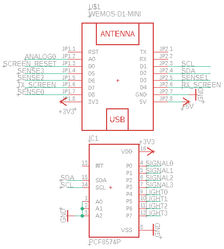
Although this seemed like an appropriate solution, it would be the cause of a lot of future problems with this version.
You will notice that there is an additional JST-XH connector and connections to D7 and D4 called T/RX_SCREEN. These connections were made after incorporating the PCF8574 and allocating the 4 relay outputs to it, I was left with excess GPIO pins (yes). This hence allowed me to dedicate 2 pins for the Nextion NX3224T024 2.4″ TFT screens which I intended to use for installing a HASPone Switch Plate.
As such the first batch of PCBs was ordered and assembled, and it was populated and bench-tested.
At first glance, everything seemed to work correctly. The switches turned on when they were turned on either via the button or the Home Assitant. Everything was looking good and so it was time for the final installation:
Alas! That was when the PCF8574 began to rear its ugly head. Immediately a huge problem encountered was that the all relays on the PCB would suddenly switch on when switching a single switch. At 0:34 I turn off the set of yellow fluorescent lights at the front, only for all the other kitchen lights to unexpectedly turn on. This was a major bug that needed squashing.
Immediately, I set to work narrowing down the cause of this unpredictable behavior. The first thing I considered was the nature of the loads being switched. I noticed that inductive loads such as fluorescent lights are more prone to this glitch, while more resistive loads such as incandescent lights were less prone. However, repeated testing found that not a single type of light was immune from this malfunction.
The next thing I did was bring the PCB back for another round of bench testing. Strangely, I was unable to replicate this glitch on the bench, which was strange since I was using similar fluorescent lamps in the bench testing. This thus suggested that the problem was due to the environment the PCB was installed in (i.e the kitchen wiring).
I posted my problem on Electronics StackExchange and obtained a few suggestions. The main issue pointed out was the lack of pullup resistors on the I2C line. This was indeed an oversight of something pretty basic and could theoretically affect the reliability of the PCF8754. Another suggestion was that the glitches were caused by transients generated when the mains is cut from the fluorescent, with the remedy being adding a varistor or a snubber diode and metal film resistor across the contacts of the relay. However, as there was already so little space in the switchbox, adding any more components would be unfeasible.
The first step I did was to solder on 4.7K pullup resistors to the I2C line, however it was to no effect. Next, I swapped out the PCF8574 but still no effect. Then, I swapped out the relay and LED lines (which involved cutting the traces and soldering wires) which allowed me to confirm that it was only the PCF8574 that was malfunctioning. This thus meant that the only solution was to remove the PCF8574 entirely. However the shortage of GPIO pins still remained. Should I replace the PCF8574 with another more reliable GPIO expander? Or perhaps there was another more elegant solution…
V2:
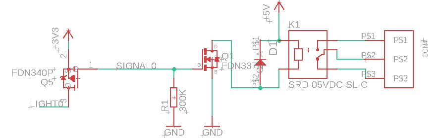
Having worked with primarily N-Channel MOSFETs due to their lower Rds, cheaper costs and better availability, I had almost forgotten about the existence of its twin – the P-Channel MOSFET. Unlike N-Channel MOSFETs, P-Channel MOSFETs are high-side switchers. That means they are placed between VCC and the load and require a negative Vgs voltage in order to be turned on (practically, this means that the source voltage has to be higher than the gate voltage, which will typically be 0V when it is ON). This essentially meant that if a P-Channel and N-Channel MOSFET had their gates tied together, the logic of the MOSFETs would be inverted (since the N-Channel would be turned ON while the P-Channel would be turned OFF at logic HIGH on the gate). Remembering that the function of the button lights was to light up when the switch was in the “OFF” position and vice versa, this configuration seemed like the optimal solution to combine two GPIO outputs into one!
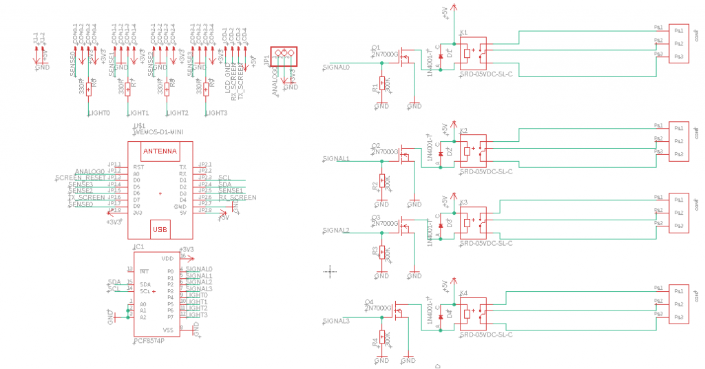
I immediately began work on V2, starting with the aforementioned MOSFET topology:
There were a few caveats, however:
- In order for the P-Channel MOSFET to turn OFF completely, the LED had to be powered from +3V3 instead of +5V (The P-Channel Vgs would be 3.3-5=-1.7V even if the GPIO was at logic high, preventing the MOSFET from turning off [unless the Vgs was significantly lower than -1.7V which in any case was risky])
- N-Channel MOSFETs typically have a pulldown resistor while P-Channel MOSFETs typically have a pullup resistor. However, we can’t possibly have both a pullup and pulldown resistor (as it would create a voltage divider). Hence, I decided to settle for a single pulldown resistor, but I found that I needed to increase the value of resistance to around 1M as lower resistances like 10K resulted in the LED not turning off completely. I think this is because there is a tiny resistance in the trace to the P-Channel MOSFET which results in a voltage divider between the GPIO pin and GND with the gate of the P-channel MOSFET in the middle of the two resistances. When the fixed resistor value is too small, the voltage at the gate of the P-channel MOSFET is ever so slightly below +3V3, causing a small amount of current to flow due to the pretty low (absolute) values of Vgs of the P-Channel MOSFET (FDN340P: -0.4V)
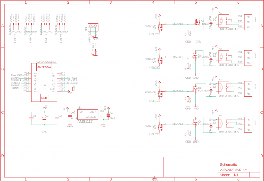
I then proceeded to test this design on a breadboard (using through-hole N- and P-Channel MOSFETs) and when it was proven to work, I ordered the v2 PCBs:
As you will notice, 8/9 of the GPIO was utilized and as such, there was no more room for the T/RX pins for the HASPone plate.
Another key difference with this design was the use of SMD components. Having designed and constructed the DIY Solder Paste Reflow Hotplate, I was really going all out with solder paste soldering due to it being faster, cleaner and more aesthetically pleasing than TO components.
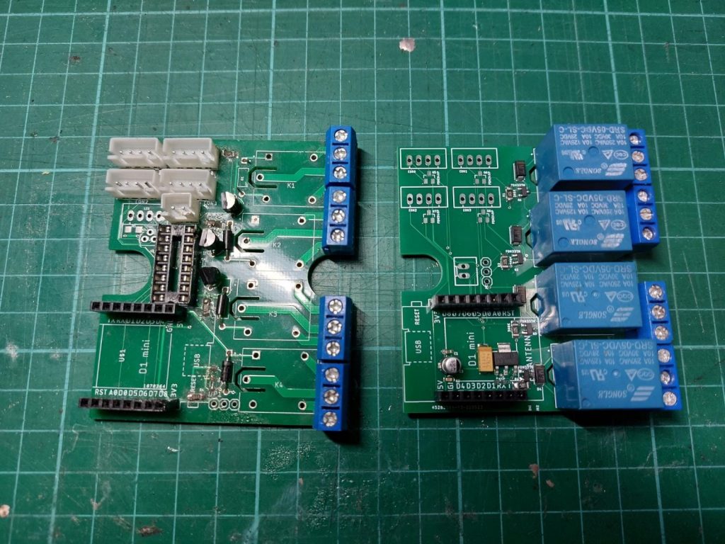
Here are V1 and V2 side by side:
Upon installation, V2 worked flawlessly. The double MOSFET configuration proved to me so much more reliable than the PCF8574. In addition, the overall board was so much cleaner and involved less components, reducing the chances of failure.
Software:
As the ESP8266s were flashed with ESPHome firmware and the automations are written in Home Assistant, the primary language was yaml which is intuitive to write and easy to understand. As mentioned relevant files are included in the GitHub Repo.
Conclusion:
Converting my home to IoT has always always been a dream of mine. As such, this project has been one massive step in that direction. With these PCBs being installed in almost all rooms in my home, the lights in my home can be remotely turned on and off either through Google Assistant or via Automations in Home Assistant. Pairing this with the recent Motion Sensors Project, the possibilities for true Home Automation abound! Here are some ideas that I have already implemented:
- Motion Sensor actuated switching on of lights when the ambient light level is below a certain threshold -> extremely useful when you forget to turn on the light or when you are carrying items and don’t have a free hand to switch on the lights (such as when I bring the dishes from the dining table to the kitchen sink)
- Motion Sensor actuated switching off of lights if no motion is detected within a certain period of time -> extremely useful when your family tends to forget to switch off the lights after leaving the room and will save energy and electricity costs in the long run.
- Google Home actuation of lights -> useful when you are too lazy to get up from your seat to turn on the lights or fan.
- One-stop turning off of all lights in the house when leaving (done usually via the HASPone TFT at the hall switch plate next to the front door)-> extremely useful when you don’t want to take off your shoes and go into each room to individually physically check that you have turned off the lights before leaving. Another plus point is that you can turn off the lights after you have left the house, hence you never need to worry about forgetting to turn off the lights.
- The list goes on…
Home automation is really a blessing [provided nothing screws up, and to be fair it hasn’t :)]. This IoT switch project is part of a long-awaited dream of mine to fully automate my home and make life more convenient for members of my household.